Pixie 2 DSB-SC Project
(Double Side Band - Suppressed Carrier)
(Double Side Band - Suppressed Carrier)
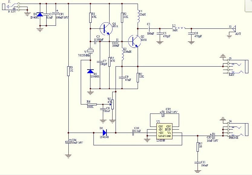
The DSBSC Pixie design stage is nearly complete. There are, no doubt, some modifications that will take place as the assembly and testing take place. As of now, the Hong Kong Pixie (Frog) will be used as a building block due to its very affordable cost and due to so many people having them already. The mods to this radio can be applied to most single conversion radios that are available. Here is the schematic of the HK Pixie:
The circuit can broken up into several modules for ease of understanding.
The circuitry that consists of Q1 and its surrounding components are a standard Colpitt's oscillator. It also contains a diode (D2) that is biased by a potentiometer (W1) that provides an automatic RIT (Receiver Incremental Tuning) function for a receive frequency offset that is desirable when using CW. The oscillator runs continuously and provides the beat frequency to the received signal (offset by the RIT circuit). In the transmit mode (KEY depressed or grounded), both sides of W1 are pulled to ground thereby removing the bias from diode D2 causing the crystal to return to its fundamental frequency.
Q2 and its surrounding components form the Power Amplifier (PA) giving this transceiver about 1 watt of output. The capacitor C4 is the connection between the two circuits. Q2 is held in the off state by C9 until grounded by the KEY at which time it turns on and applies the amplified RF to the antenna. C4 is where we will interrupt the circuit to install a Double Side Band Suppressed Carrier (DSBSC) circuit for modulation.
U1 (LM386) is the audio amplifier. The Colpitt's oscillator and the received signal are mixed in U1 to complete the single conversion process and produce an audio signal.
L2, C5, and C6 form a PI filter for the output RF to reduce out-of-band harmonics.
MODIFICATIONS:
NOTE: The reference designators for the parts in the following schematics are different than the Master Pixie schematic above. The schematic drawing program used to create the modifications automatically sets the designators and they have not been changed to match the original schematic yet. It is a cumbersome task, but I will eventually get around to doing it. Just match the parts in the changes with the parts shown in the original Master HK Pixie schematic. If you prefer not to use the HK Pixie but would rather build from scratch, the complete schematic is below.
To start with, we will remove the crystal (Y1), the potentiometer (W1), and the coupling capacitor C4. The circuit below will then be added with a panel mounted 4PDT push button switch (S3) to control the transition from receive to transmit for voice and digital modes. The RF in (S3a common) is connected to the Colpitt's oscillator side of where C4 used to be installed and the RF/DSB out (S3b common) is connected to the side of C4 that went to the power amp. S3 is shown in the normally closed position in all of the schematics. S3a and S3b normally closed (N.C.) positions are connected to each other. The normally open sides of S3a and S3b are connected to the modulator RF in and the DSBSC out respectively. The modulator itself (as well as the mic amplifier) can be constructed pad or Manhatten style (or other method) depending upon your preference.
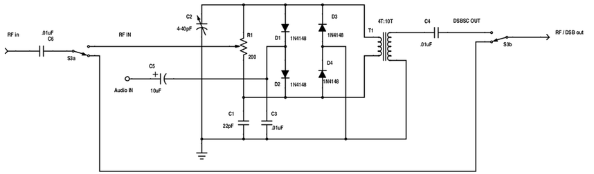
The DSBSC modulator is balanced using C2 and R1 to suppress any carrier bleed through caused by the imbalance of the diodes in the ring modulator.
The next step will be to modify the Colpitt's oscillator for RIT, VXO, and standard operations (selectable). The schematic is below:
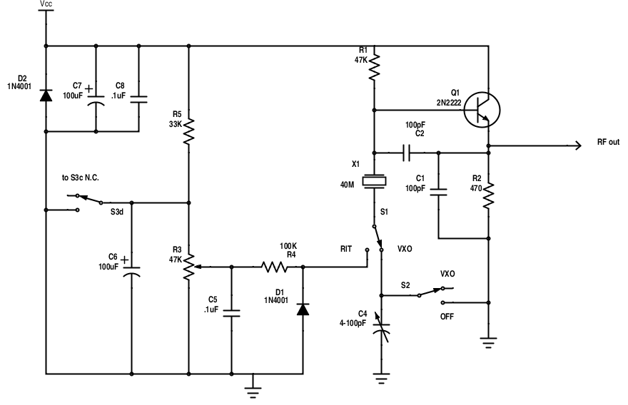
Where the crystal was pulled out, add a wire to the side that was connected to the base of transistor Q1 that is long enough to reach the panel mounted switch S1 (RIT/VXO). Solder one side of the crystal that you intend to use (or a crystal holder socket) to the common of switch S1 and the other side of the crystal holder to the wire coming from the base of Q1. Now solder a wire from one of the switched sides of S1 (that you will use as the RIT function) to the other side of where the crystal Y1 was removed. The other side of S1 (the VXO side) will go to a panel mounted variable cap (C4 in the schematic shown) and the other side of the variable cap goes to circuit ground. Panel mounted switch S2 common will go to the panel mounted ungrounded side of C4 and the OFF side of the switch is connected to circuit ground. You will also panel mount a 47K ohm potentiometer (R3) and wire the corresponding connections for the variable tape and the ground to the location on the board where you pulled the small RIT potentiometer out. The other side of the potentiometer is connected with a 33K ohm resistor to the Vcc power supply (found at the positive side of C7). Finally, the common of S3d is connected to the ungrounded side of the R3 potentiometer (that has the 33K ohm resistor), the N.C. side (Normally Closed) of S3d is connected to the N.C. side of S3c and the N.O. (normally open) side of S3d is connected to circuit ground.
Now we have a few changes to the Power Amplifier stage. The schematic is below:
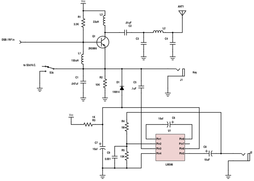
The last change to the circuit is the common connection of switch S3c goes to the pad on the circuit board that is still empty where the RIT potentiometer was removed. This can be double checked by ohming it out with a meter to the junction of L1 (L3 on the original schematic) to insure proper connectivity. The N.O. side of S3c goes to circuit ground and the N.C. side is already connected to S3d N.C.
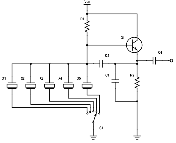
If you would like to have several crystals on a panel mounted rotary switch for ease of frequency change, you can use the circuit below as a guide to installing one in place of the fixed crystal shown above. Just install the switch with crystals in place of the single crystal that is shown.
If you would like to have several crystals on a panel mounted rotary switch for ease of frequency change, you can use the circuit below as a guide to installing one in place of the fixed crystal shown above. Just install the switch with crystals in place of the single crystal that is shown.
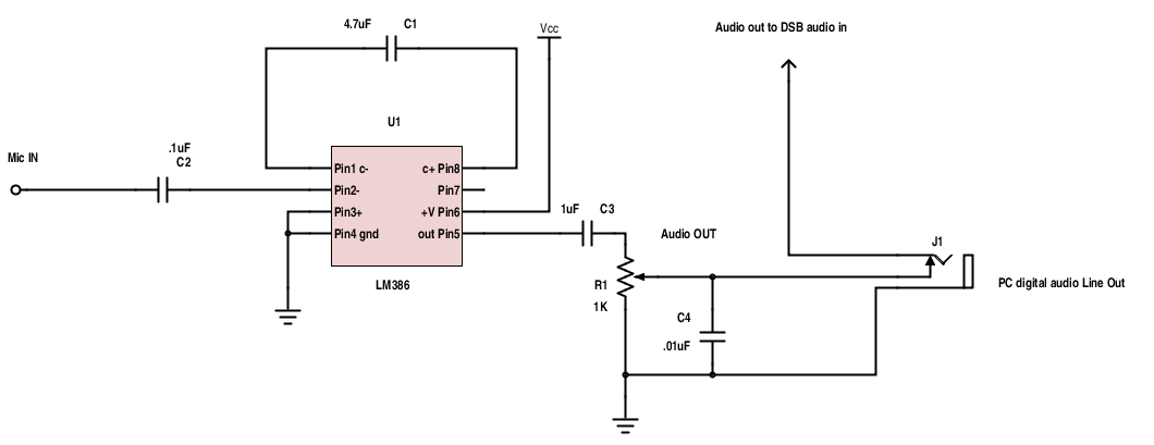
To adjust the DSBSC modulator for proper use, connect the antenna output to a dummy load and depress the PTT (S3) button. Alternately adjust the potentiometer R1 and the capacitor C2 until you do not see the carrier on the waterfall of a setup connected to another radio (an existing setup, if you will). For a voice operation in DSBSC mode, you will need to add the following circuit that includes a jack for a PC to send digital modes:
Update (4-20-15)
To boost the output of the LM386 audio amp, disconnect pin 2 from the ground by lifting the pin or cutting the trace (depending on your board version). Place a 1Meg resistor from pin 2 to the negative (-) side of the audio output cap (CP3 in the original HK Pixie schematic). Place a 15K resistor from pin 2 to ground. Also, place a .001 cap from pin 2 to ground (prevents oscillations). Your gain should be much better with this mod. The schematic of the Power Amplifier stage now shows these changes.
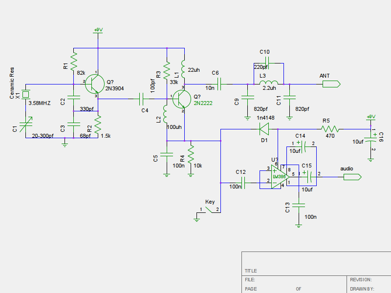
The complete schematic is below:
To boost the output of the LM386 audio amp, disconnect pin 2 from the ground by lifting the pin or cutting the trace (depending on your board version). Place a 1Meg resistor from pin 2 to the negative (-) side of the audio output cap (CP3 in the original HK Pixie schematic). Place a 15K resistor from pin 2 to ground. Also, place a .001 cap from pin 2 to ground (prevents oscillations). Your gain should be much better with this mod. The schematic of the Power Amplifier stage now shows these changes.
The complete schematic is below:
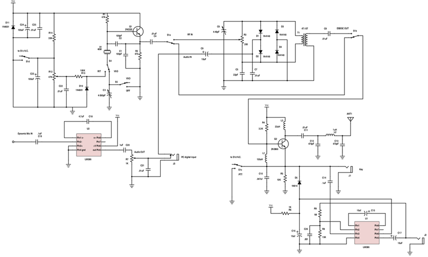
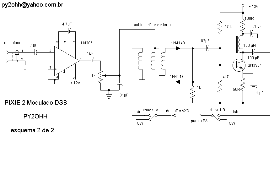
Below are some additional circuits for a Pixie with a VXO and a different DSBSC circuit.
|
|
